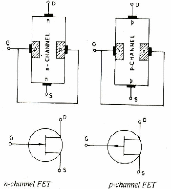
The junction transistor, the best known type, led to the solid state electronics revolution. It has the disadvantage of a low input impedance because the base of the transistor is the signal input and the base-emitter (the output) diode is forward biased. Another device achieved the same result, of using a small signal input to control a much larger output with the input diode junction reversed biased, and this device is called a "field effect transistor". With the reverse biased input junction, it has a very high input impedance. Having a high input impedance minimizes the interference with or "loading" of the signal source when a measurement is made, but the field effect transistor is limited in the frequencies it can operate at.

The main parts of a field effect transisttor are:
-
The source S where the majority charge carriers enter the transistor.
-
The drain D, where the majority charge carriers leave the transistor.
-
The gate G, the heavily doped p or n type region.
-
The channel, through which the majority charge carriers move between sourvce and drain.