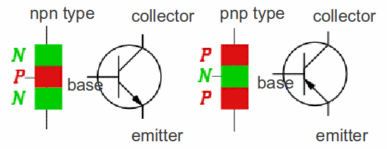
The transistor consists of three layers of semiconductor material. Transistors come in two types – either npn, consisting of a layer of semiconductor material in which the majority charge carriers are positively charged 'holes' between two layers of semiconductor material in which the majority charge carriers are negatively charged electrons, or pnp, consisting of a layer of semiconductor material in which the majority charge carriers are negatively charged electrons between two layers of semiconductor material in which the majority charge carriers are positively charged 'holes'.

The layer of semiconductor material in the middle is called the base, and the layers at either side are called the emitter and the collector. The base is very lightly doped (consists of more nearly pure silicon) than the emittor or the collector, and is only a few millionths of a meter thick (about 3-5 micrometre).
The emitter base junction is always forward biased – so that the applied voltage is in the direction of the charge carriers) and the base collector junction is always reverse biased (so that the applied voltage is against the charge carriers).
Concentrating on the npn transistor, when the base emitter voltage is about 0.6 V or more, current will flow. Electrons will flow through the base from the emitter to the collector. No current will flow without this base emitter voltage, since it is needed to overcome the reverse bias voltage between the emitter and collector.
The emitter current is the sum of the collector current and the base current, with the collector currnet being about 100 times more than the base current.
